CMOS Imager Design in Cadence
April 2022
EN.520.216 Introduction to VLSI
Objectives:
Skills Applied & Outcomes:
Comments:
I sketching and designing layouts on paper and in the software, debugging, and writing the report. We made a few mistakes at the beginning but managed to fix them by the end of the project.
5T amplifier layout.
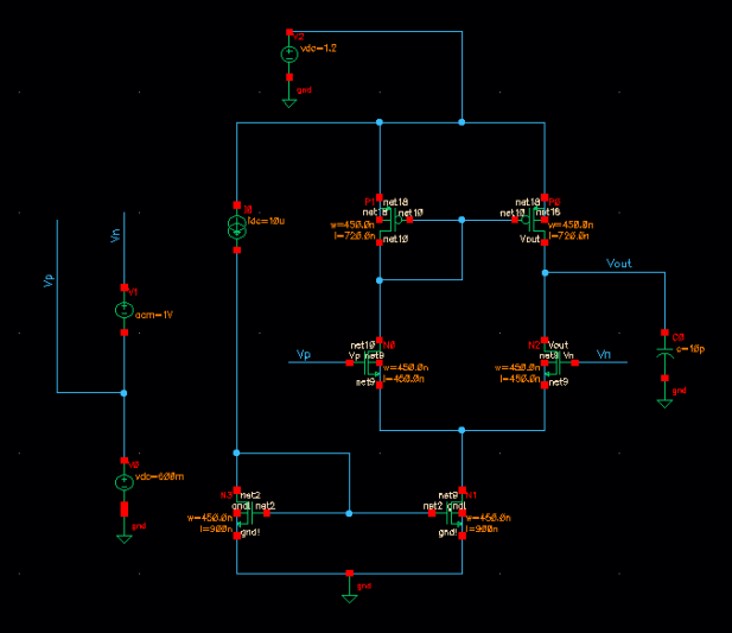
5T amplifier schematic.
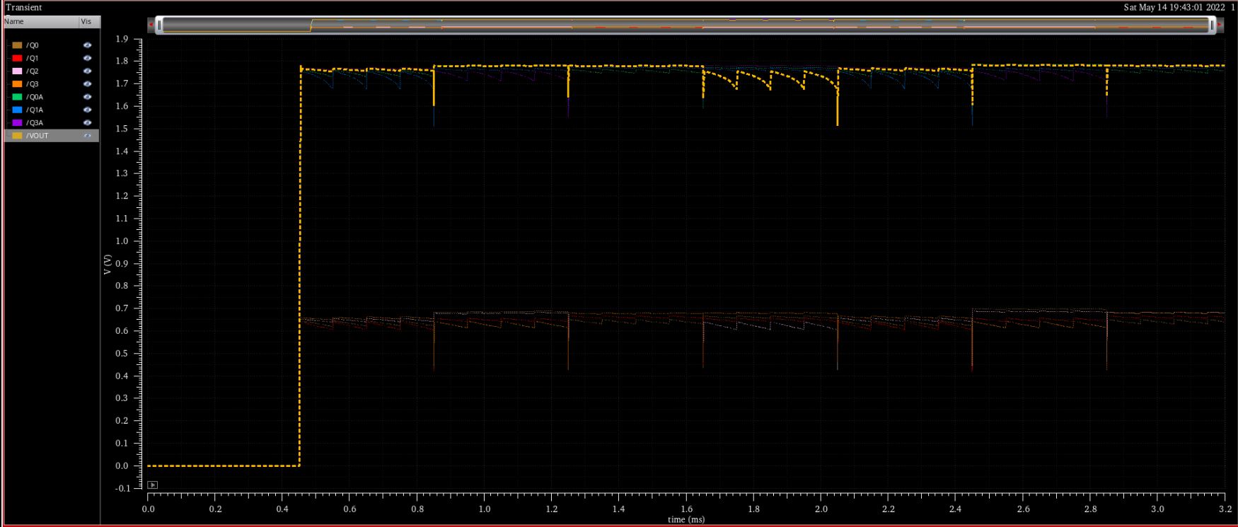
Sample voltage output of 16 photodiode cells in an array.
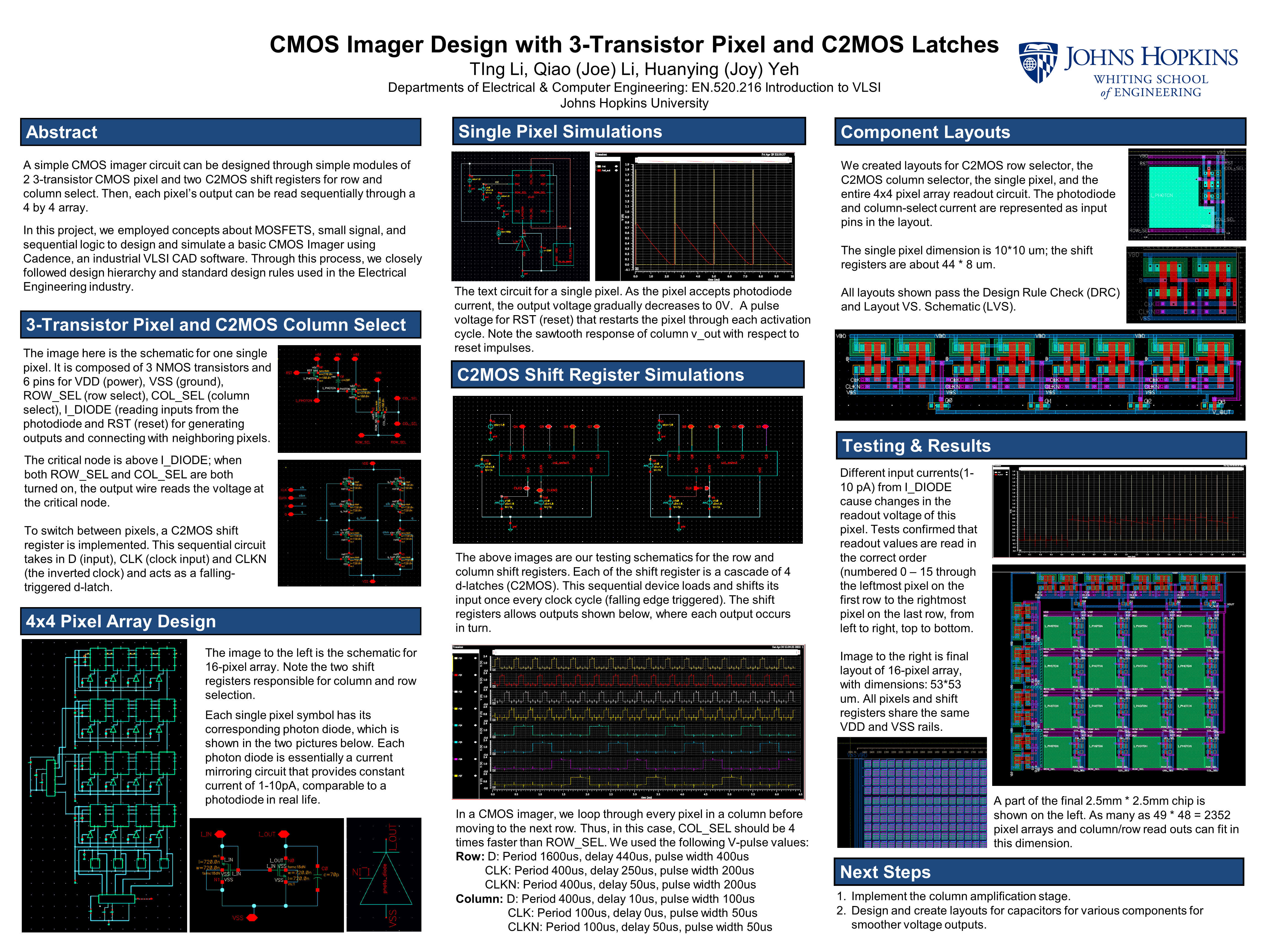
the 2022 JHU Design Day Poster. Click image to enlarge.
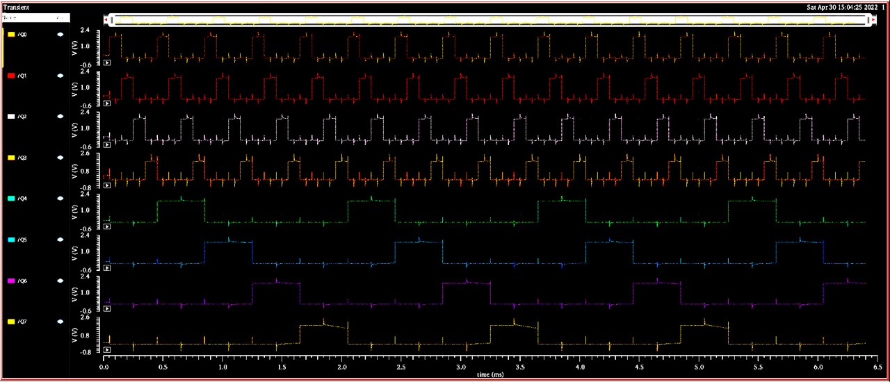
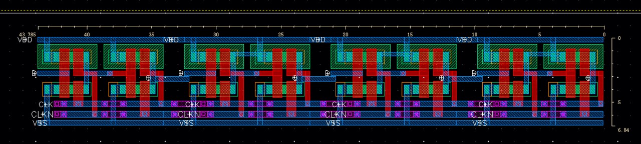
C2MOS shift register simulations to control a 4 x 4 array.
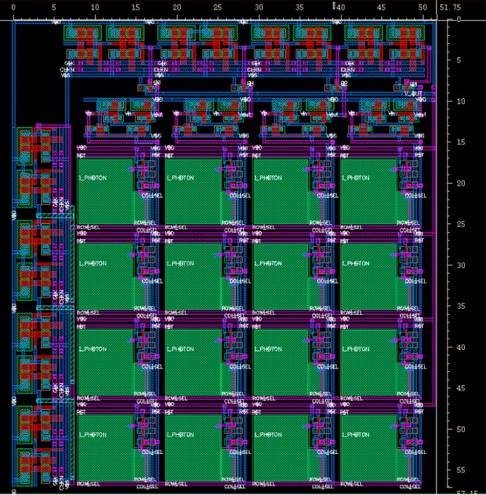
The 4x4 imager chip layout with column amplifier.